


[065] Flyback Development Part II - Initial Testing
Flyback design bias and control circuit testing with high voltage.
Introduction
This article is the second of a series in which Dr. Ridley shows the steps involved in designing and building an offline flyback converter. The second part of the series begins testing on the bias and control circuit, and verifies the high-voltage operation of the power FET with a resistive load.
Initial Bias and Control Chip Testing
The specifications of the flyback power supply were given in Part I of this article [1]. Figure 1 shows the full schematic of the flyback power converter with the control, bias, and power stage blocks. All parts of the circuit are fed directly from the rectified ac input line.
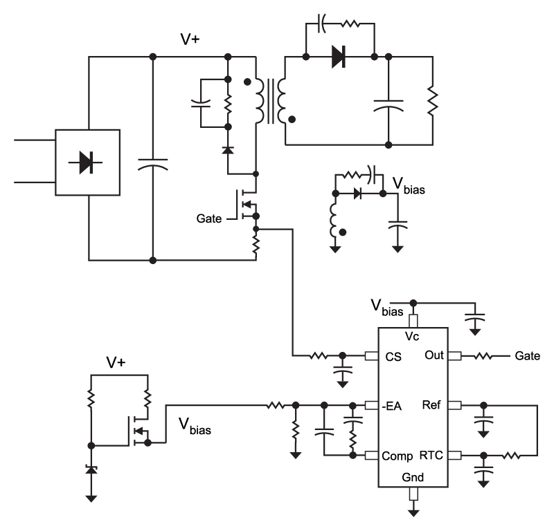
Figure 1: Full schematic of a flyback converter.
The most complex part of the converter is the transformer, and its design will impact the noise, regulation, and efficiency. Before this is placed in the converter, however, it is a good idea to test the primary side control, bias, and switching with the full input line voltage. This will reveal design flaws that can be remedied before the transformer is inserted.
Figure 2 shows the schematic of the flyback power supply system with the transformer replaced with just a load resistor. For efficient initial design and testing of low-power supplies, it is a good idea to put sockets on the board for the transformer. This allows multiple transformer design ideas to be quickly tested and compared, as we will see in the future parts of this design series. Plugging a load resistor into the primary-side sockets allows some meaningful power testing to begin.
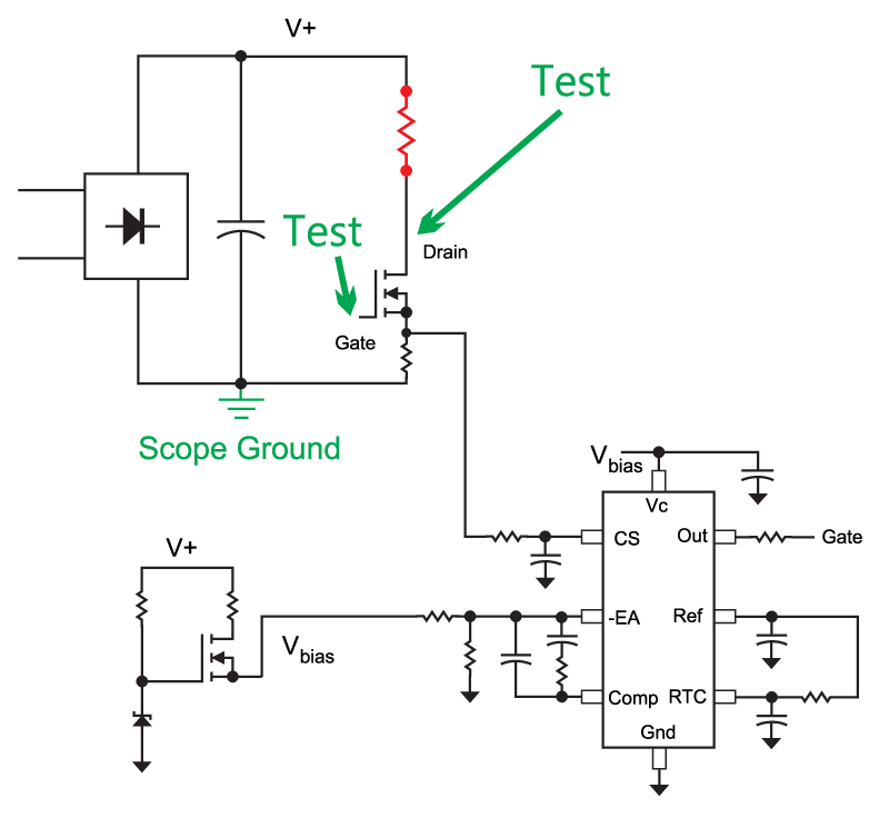
Figure 2: Schematic of flyback converter with transformer replaced with load resistor.
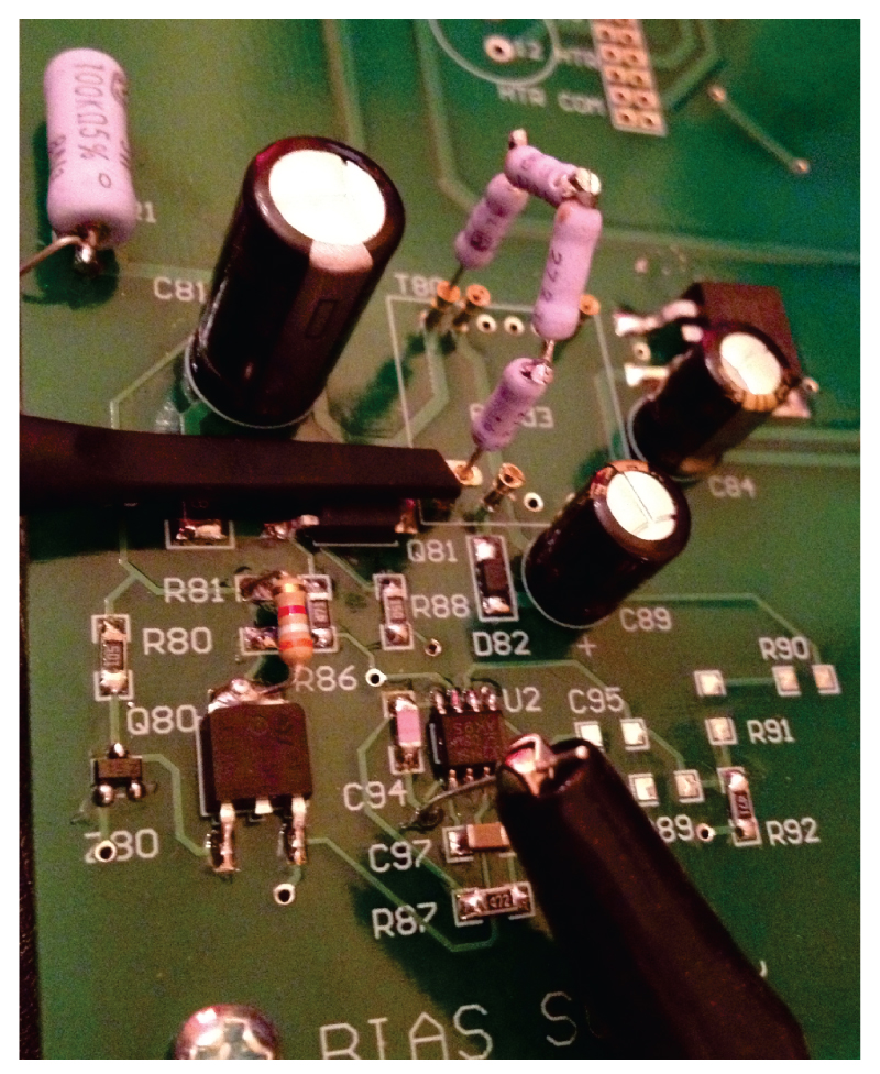
Figure 3: Photograph of flyback converter circuit board with load resistor plugged into transformer sockets.
Initial voltage is applied to the input to make sure the bias circuit is operating properly. For this test, the resistor in the transformer sockets is removed, and a dc bench supply is used to apply up to 60 V. As the input voltage is increased, the gate voltage on the bias FET increases until it is regulated at 15 V by the zener diode. The source of the bias FET provides voltage to the control chip, and when the start threshold of the chip is reached, the gate drive signal seen in Figure 4 can be observed.
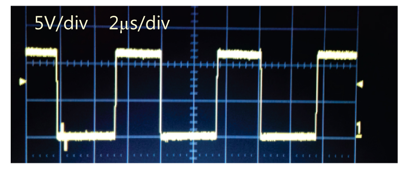
Figure 4: Flyback converter gate drive signal.
Once the control chip starts switching, current is drawn through the 1.8k resistor, and the chip bias will reduce. The intent of this resistor is to reduce the initial surge current through the bias FET when high voltage is suddenly applied. A through-hole resistor is used for this component since it can have high initial current and voltage, and in the event of a power supply fault, the dissipation can be significant. (When the transformer is in place, the bias network will shut off when the auxiliary voltage is above approximately 12 V, and the dissipation in the bias circuit resistor will greatly stop.)
Once the gate drive waveforms are verified, it is a good idea to test the circuit up to the full input voltage. As described in [2], an isolated ac source is a recommended method of performing initial testing and design of converters. Figure 5 shows a 1-kW isolation transformer and variac used to apply high voltage to the circuit. This test setup is easy to build, and provides flexibility for grounding the flyback circuit during testing.
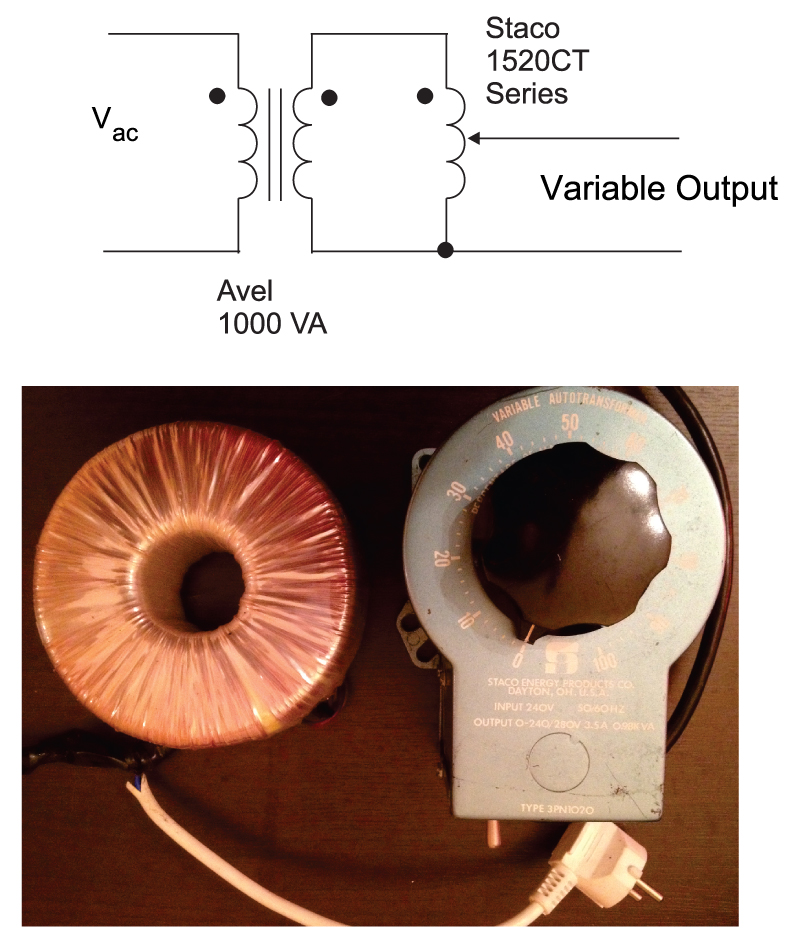
Figure 5: Isolation transformer and variac used to apply full line voltage to converter.
The input voltage was increased to 300 VAC to thoroughly test the bias and control circuit. Testing at high voltage was done in short bursts since the 1.8k resistor dissipation is high and cannot be sustained for long periods of time.
FET Switching Waveforms
The load resistor was then plugged back into the sockets of the transformer to test the switching of the power FET. An initial value of 5.6k was used and this allows testing up to an input voltage of about 120 VAC. Beyond that, the dissipation is too high, and the resistor was changed to a 10 k value with a continuous power dissipation capability of 5 W.
Figure 6 shows the drain waveform on the FET with these two different loads. In the first plot, the circuit sees a dc input voltage of 280 V. The dissipation is about 7 W in the power resistor, but this was applied for a short duty cycle.
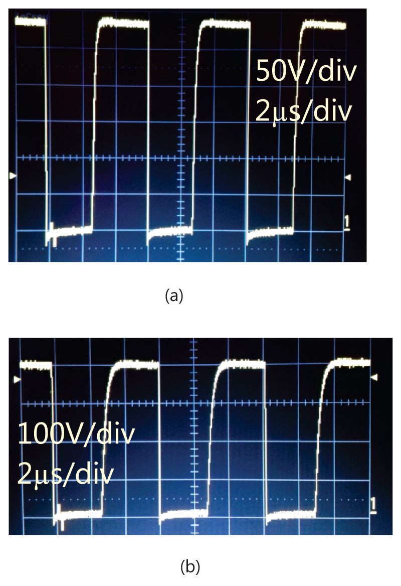
Figure 6: Flyback converter drain signal with (a) 5.6k load and 190 VAC input; (b)10k load and 280 VAC input.
The second plot of Figure 6 shows the drain waveform with a 400 V dc input and a 10k load. The large value of resistor results in a slow rise time on the FET as the output capacitance takes a significant time to charge.
Figure 7 shows the drain waveform with the lowest line input at which the flyback converter controller will operate without experiencing dropouts. This occurs with a minimum dc input voltage of 60 V, seen at the bottom of the input capacitor ripple. A lower value of the 1.8k resistor will reduce this minimum voltage, and a higher value will increase it. It is important that the bias supply keeps running at the lowest possible input line for the converter in order to get the output into regulation at low line.
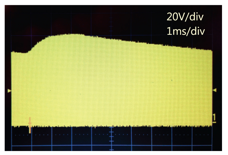
Figure 7: Flyback converter drain signal at lowest line for continuous operation. Minimum dc voltage level for continuous operation is 60 V.
Summary
Initial testing has been done on the circuit with the transformer replaced with a power resistor. This allowed verification of the bias circuit, control chip, and switching of the FET with a significant load and the full input voltage. This type of initial testing, without having the complications of a transformer, is very useful for finding circuit design and build problems on the primary side. It is important to do maximum input voltage testing early on in the prototype development to find any design flaws.
In the next part of this series, we will look at the design of the power transformer.
References
- Join our LinkedIn group titled “Power Supply Design Center”. Noncommercial site with over 7000 helpful members with lots of theoretical and practical experience.
- For power supply hands-on training, please sign up for our workshops.
- "Flyback Power Supply Development Part I", Power Supply Design Center.
- "Testing Off-Line Power Supplies", Power Supply Design Center.
- www.ti.com/product/uc3842, control chip datasheet.