


[024] Frequency Response Measurement Part 2: Single-Frequency Measurement
Single-frequency injection and measurement is used to analyze and test power supplies.
Introduction
In this article, Dr. Ridley continues the topic of frequency response of switching power supplies. Last month’s article focused on the broadband noise generation of power supplies. This article shows how we can extract single frequencies one-by-one from the noise with the AP300 frequency response analyzer. This allows us to perform control measurements on our switching power supplies.
Single Frequency Measurements for Switching Power Supplies
The previous article in the Design Tips series of this magazine [1] discussed the wide range of frequencies generated by a switching power supply. High noise is unavoidable when working with switchers, and the converter must also be tightly controlled in the presence of this noise.
This presents a challenge in two areas: firstly, the control chip must run reliably with the noise and predictably set the duty cycle of the switch from one cycle to the next. Secondly, measurements must be taken on the power supply once a control loop is closed to ensure that it is always stable.
Analog controllers do an excellent job of managing the first problem through the simple sawtooth ramp and reference technique of a standard PWM controller. Once the controller is working properly, we use traditional Bode plot measurements to assess performance and stability.
Power supplies are one of the few areas of analog electronics that still make conventional measurements rather than depending on prediction and modeling alone. The loop gain and stability margin can vary tremendously for a converter operating over its full range. Figure 1 shows the range of variation that can exist for a simple buck converter when variations of line, load, temperature, and EMI filter are considered.
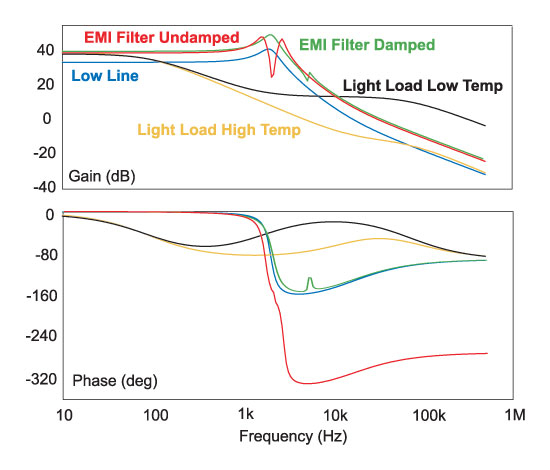
Figure 1: Variability of Bode plots for a “simple” buck converter with variations of line, load, temperature, and EMI input filter.
These curves show extreme changes in the gain and phase of the converter. The curves, however, assume linearized operation, with small-signal circuit models used to generate the plots. In the real world, the switching power supply may have regions of operation that are not well modeled, and even more variation is possible. Clearly, in the face of such extreme behavior, measurement of the power supply is an essential step in making sure the design of the control loop is rugged.
Figure 2 shows a typical noisy power supply waveform with an injected signal, used to make control measurements. This points out another unique requirement of switching power supplies – specialized equipment is needed to be able to extract the injected waveform in the presence of the switching noise. This is done with a frequency response analyzer.
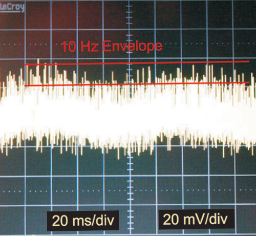
Figure 2: Typical power supply waveform with signal and noise.
Frequency Response Analyzer
A frequency response analyzer is a piece of test equipment designed to inject a sinewave into a circuit, and measure the response of the circuit at that single frequency at two different test points in order to generate a gain and phase response. The injected sinewave is swept from frequencies as low as 0.1 Hz, up to the switching frequency of the converter.
The role of the frequency response analyzer is to extract extremely small test signals (sometimes much less than 1 mV) from noisy waveforms, and compare their gain and phase. The technology needed to do this is not new, having been used for decades in our field.
Figure 3 shows a block diagram of the AP300 analyzer which is designed for switching power supplies. An oscillator puts out a test signal which is injected into the circuit to be measured. (Techniques for injection will be presented in later articles in this magazine.) Two input channels on the analyzer are used, connected to different test points in the circuit. Each input channel processes a test signal, first with analog signal processing to eliminate noise, then with digital signal processing. The output of the digital processor interfaces with a computer.
The analog section of the input channels work in a similar way to radio receivers, using wide band amplifiers, and heterodyning techniques with mixers and filters to isolate the test signal, and reduce the frequency of the carrier down to an easily measurable quantity. Communication theory tells us that the gain and phase of the test signals can be preserved when producing an IF bus in this manner. This greatly simplifies the task of the A/D conversion stage of the system.
After A/D conversion, the data is passed to a microprocessor, and then to a computer to perform further digital filtering and noise reduction. The results can then be presented as a traditional Bode plot to the user.
Using these techniques, the AP300 achieves extreme values of signal-to-noise and dynamic range, in excess of 110 dB. This is essential for reliable measurement of switching power supplies. Further details of the theory are given in [2].
This process cannot be short-circuited with modern “frequency-response analyzer on a chip” products that have recently been introduced. The integrated chips for this have neither the dynamic range, or noise-rejection capability needed for switching power supply measurement, although they may work reasonably well for linear, non-switching circuits where noise levels and gains are low.
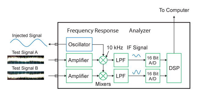
Figure 3: AP300 Frequency response analyzer test equipment block diagram.
Using the frequency response analyzer, individual frequencies are extracted from the noise, and two signals can be accurately compared in terms of gain and phase. This allows us to study the control characteristics of a system and design the feedback loop properly.
Summary
The frequency response analyzer is a highly specialized instrument that we use, and it is essential for stabilizing power supplies quickly and efficiently. In the next two articles in this series, the essential role of loop gain measurements will be discussed and compared to the technique of trying to design control loops with step-load response measurements.
References
- Join our LinkedIn group titled “Power Supply Design Center”. Noncommercial site with over 7000 helpful members with lots of theoretical and practical experience.
- For power supply hands-on training, please sign up for our workshops.
- “Frequency Response of Switching Power Supplies”, Power Systems Design Magazine, Design Tips Archive, January 2009. http://www.powersystemsdesign.com